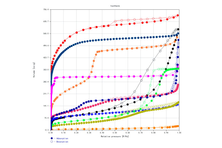

As core materials for solar cells, thin-film transistors, and other optoelectronic and semiconductor devices, the performance and quality of polycrystalline and amorphous silicon thin films largely depend on their microstructure and physical properties. Testing the specific surface area and true density is crucial for a deeper understanding and optimization of these materials. A larger specific surface area implies more active sites on the material's surface, beneficial for light absorption and carrier generation and separation in solar cells, thus enhancing the photoelectric conversion efficiency. Meanwhile, in thin-film transistor applications, an appropriate specific surface area helps improve carrier mobility and device switching speed. True density testing provides important evidence for assessing the quality of polycrystalline and amorphous silicon thin films. It reflects the compactness and uniformity of the internal structure. High true density silicon thin films usually exhibit better electrical performance and stability, reducing carrier recombination losses, and improving the efficiency and lifespan of solar cells. In thin-film transistor applications, accurate true density data aids in optimizing film thickness and uniformity control, ensuring device consistency and reliability. Testing the specific surface area and true density of polycrystalline and amorphous silicon thin films is key to gaining a deep understanding of material characteristics, optimizing preparation processes, and enhancing device performance and quality, which holds significant practical implications for driving technological advancements in the optoelectronic and semiconductor industries.
contact
Be the first to know about our new product launches, latest blog posts and more.Any question or request?
Click below, we’ll be happy to assist. contact